



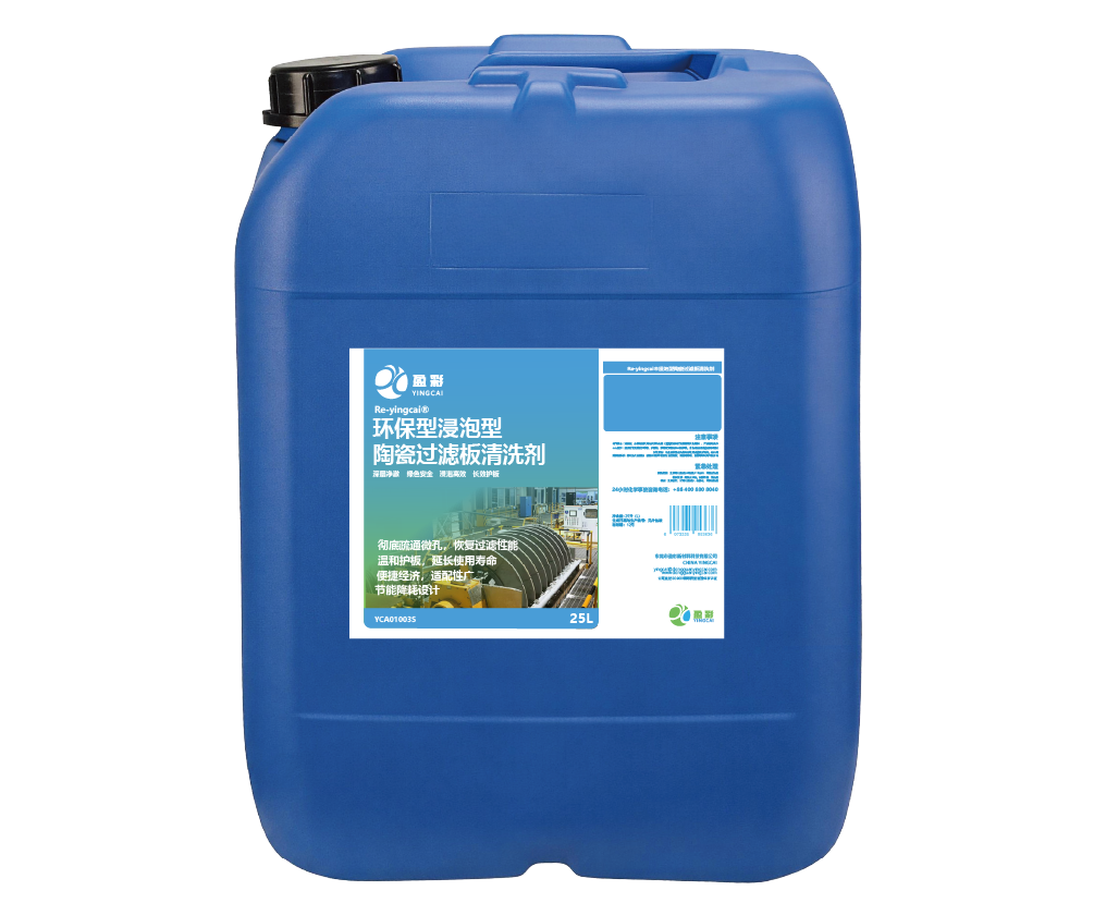










Cases
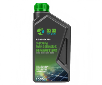
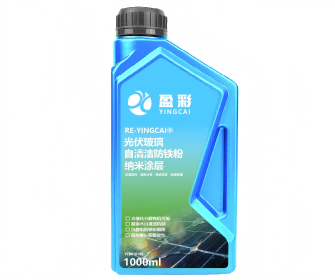
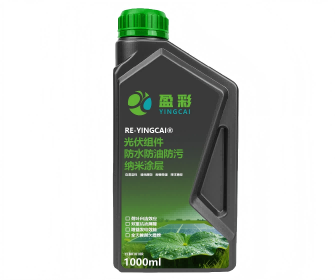
Not only used on photovoltaic panels

-

 System
Customized Precision Cleaning System
-
 Place
PlaceTangxia Town, Dongguan, Guangdong, China
-
 Date
Date2025-11-15
-
 Application
Yield Improvement, Precision Cleaning, Semiconductor Chip Cleaning, Wafer Surface Cleaning, Residue Removal and Process Stability Enhancement
Project background
During the mass production of 7nm logic chips, the customer faced several cleaning-related process challenges that affected yield stability and product performance consistency.
The main issues included water mark defects on the sidewalls of FinFET three-dimensional structures after cleaning, nanoscale residues after EUV lithography, unstable contact resistance, and uneven cleaning at metal gate interfaces. These problems increased defect risks, caused parameter fluctuation, and made product consistency difficult to control.
To solve these challenges, YINGCAI developed a staged and customized precision cleaning solution focused on residue removal, surface protection, process stability, and yield improvement.
Project introduction
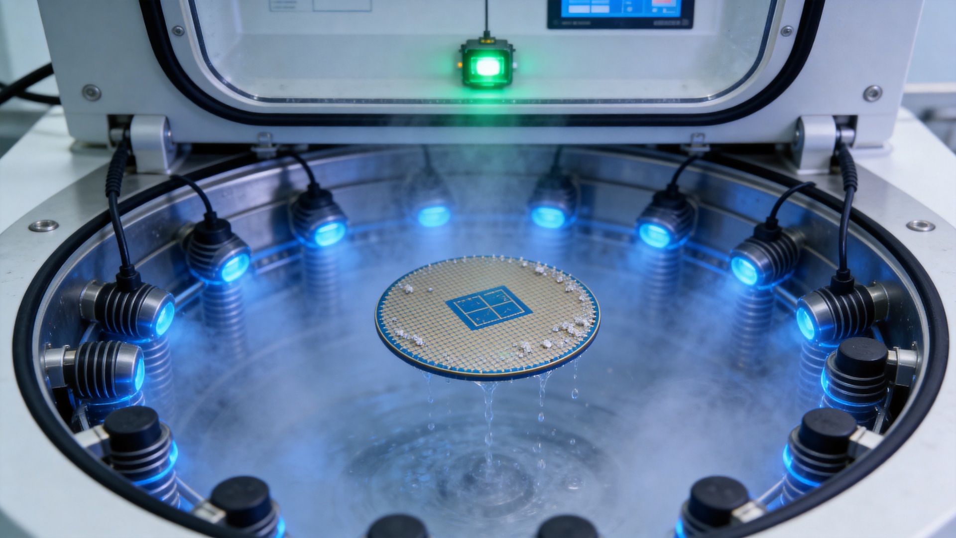
YINGCAI designed a multi-stage precision cleaning process according to different contamination types and process requirements.
Stage 1: Precision Cleaning after EUV Lithography
A microbubble-enhanced SPM cleaning process was used to improve photoresist residue removal. The process achieved a photoresist removal rate of over 99.99% while maintaining high wafer surface quality and providing a clean foundation for subsequent processes.
Stage 2: Non-Destructive Cleaning for FinFET Structures
A low-pressure atomized cleaning process was applied to reduce water mark defects on Fin sidewalls. The cleaning process protected delicate structures and controlled dimensional change within 0.5 nm, helping achieve non-destructive cleaning for advanced semiconductor structures.
Stage 3: Interface Cleaning for Device Reliability
Ultra-low-concentration chemical cleaning combined with megasonic-assisted technology was used to remove metal ion contamination and improve interface cleanliness. The solution reduced metal ion contamination to below 5×10⁹ atoms/cm² and helped improve device reliability and electrical performance consistency.
Extended Application: Third-Generation Semiconductor Cleaning
The solution was also extended to SiC and GaN semiconductor materials. For SiC power devices, a dedicated post-CMP cleaning solution helped reduce surface defect density. For GaN RF devices, a precisely controlled cleaning and stripping process improved surface cleanliness while enhancing surface flatness.
Customer value
After implementation, the project achieved significant improvements in yield, performance consistency, process efficiency, and sustainable manufacturing.
Yield Improvement:
During a 12-month mass production period, the overall chip yield increased from 92.1% to 95.7%, improving by 3.6 percentage points.
Performance Stability:
The consistency range of key chip performance parameters improved from ±8% to ±3%, making product quality more stable and reliable.
Operational Efficiency:
The preventive maintenance cycle of key equipment was extended from 2 weeks to 4 weeks, improving equipment utilization and reducing process interruption.
Cost Reduction:
While improving cleaning performance, the cost of specialized cleaning chemicals was reduced by approximately 28% compared with the original process.
Sustainable Manufacturing:
More than 90% of cleaning chemicals were recycled and reused, helping reduce wastewater discharge pressure and overall resource consumption.
Technical Support:
YINGCAI provided process optimization, technical training, data follow-up, and continuous improvement support, helping the customer build a more stable cleaning process for advanced semiconductor manufacturing.
Product Inquiry
-
Purchase products
-
Become a partner
-
After-sales service

-
1.Project background
-
2.Project introduction
-
3.Customer value
-
4. Product Inquiry


